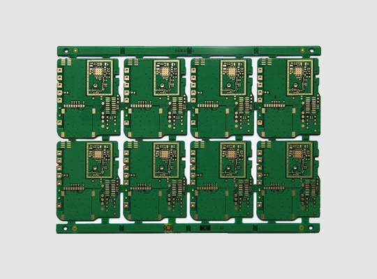
8L 2+N+2 ENIG
HDI circuit board advantages:
1. Reduce PCB cost: when the density of PCB increases more than eight layers, it will be manufactured with HDI, and the cost will be lower than that of the traditional complex pressing process;
2. Increase circuit density: interconnection between traditional circuit board and parts;
3. Conducive to the use of advanced construction technology;
4. Better electrical performance and signal correctness;
5. Better reliability;
6. Improve the thermal properties;
7. Improve RF interference, electromagnetic interference and electrostatic discharge (RFI/EMI/ESD);
8. Increase design efficiency.
| Layer Count | 4L-18L mass production, 20L-50L quick-turn |
| Material | High Tg material |
| Finished Board Thickness | 0.8-4.8mm |
| Finished Copper Thickness | Hoz-8oz |
| Max. Board Size | 600X8000mm |
| Min. Drilling Size | 0.15mm, 0.1mm(laser drilling) |
| Blinded hole depth ratio | 1:1 |
| Min. Line Width/Space | inner 2/2mil, outer 3/3mil |
| Surface Finish | ENIG, Immersiong Silver, Immersion Sn, Plated Gold, Plated Sn, OSP ect. |
| Standard | IPC Class 2, IPC Class 3, Millitary |


